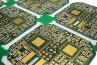
Printed Circuit Board Design
Ionocom offers design of printed circuit boards as part of the product development process. We can also offer this as a standalone service.
Our experience ranges from single-sided boards designed for absolute minimum cost to high-performance multi-layer boards with power and ground planes designed for RF, high-speed and high-density situations.
- High-volume products where routing the design on a two-layer (or even single-sided) board is important to reduce costs.
- Analog circuits where careful attention to routing and grounding is required to reduce noise and interference.
- Radio frequency circuits where trace impedances must be controlled.
- Digital logic circuits where grounding and screening is important to reduce EMI emissions.
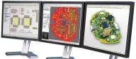
CAD
Our primary CAD tool is Altium Designer. In addition to excellent schematic capture and printed circuit board layout tools this provides us with 3D mechanical integration, allowing visualisation of boards, components, enclosures and other mechanical parts, and exchange of mechanical data in industry-standard formats.
Ionocom is an Altium partner and an official Altium Design Center.
In addition to Altium Designer we have extensive experience with Cadence OrCAD Capture and Layout. We use OrCAD for maintenance of existing designs. We also have KiCad available for customers who prefer open-source tools.
We typically perform both placement and routing by hand for the best results. We use automated design rules checking and extensive in-house checklists to ensure that designs are correct and manufacturable. We design PCBs to be produced to IPC A 600 standards.
Next: Software design